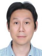
巫勇賢
近期热点
资料介绍
个人简历
PhD, National Chiao Tung University
Research Statement
The microelectronics sector has spurred a global information revolution through the persistent drive to make semiconductor devices faster, smaller and cheaper. For the past four decades, the minimum feature size employed to fabricate integrated circuits have exponentially decreased and the corresponding enhancement in transistor performance is also achieved. The catalyst at the heart of this progress has been a relentless pursuit of advances characterized by the famous “Moore’s Law” observation.
Professor Hugo De Man, co-founder of IMEC, has identified the period from 1980 to 1995 as the era of “happy scaling” since simple transistor miniaturization went hand in hand with higher performances and lower costs and brought in the proliferation of ASICs. However, these euphoric days are over and concomitantly we are confronted with the difficulties to achieve performance improvement as MOS devices approach scaling limits. Aiming at the phenomenon that size and speed of future chips would eventually slow down because of the limits of silicon, Gordon Moore, co-founder of Intel, remarked ”No exponential forever. But you can delay forever.” We are now at the critical juncture in silicon technology innovation. What can we do to delay forever?
Strained silicon and high-k gate dielectric are the hottest solution to overcome this difficulty. For strained silicon, SiGe is the well-known material to introduce strain to the MOS device, what else is there to study for SiGe? Is strained silicon the ultimate option for channel material of MOS device? For high-k materials, besides logic devices, what is its impact on the performance of memory device? To learn more about these topics, please directly contact me or visit my website.
ESS department has an excellent history and devoted to Expand the possibilities, Stimulate the technologies and Shape the future by perpetual thinking and research. If you are desperately striving for excellence and pleased to face work that is challenging and creative, come join us!
研究领域
•Ge-Based Devices
•Memory Process Development
•Nano-Device Characterization""
近期论文
1. Kuen-Yi Chen, Pin-Hsuan Chen, and Yung-Hsien Wu*, “Excellent Reliability of Ferroelectric HfZrOx Free from Wake-Up and Fatigue Effects by NH3 Plasma Treatment,” in Symp. on VLSI Tech., Kyoto, Japan, 2017.
2. Yung-Shao Shen, Kuen-Yi Chen, Po-Chun Chen, Teng-Chuan Chen and Yung-Hsien Wu*, “Flash Memory Featuring Low-Voltage Operation by Crystalline ZrTiO4 Charge-Trapping Layer,” Scientific Reports, vol. 7, p. 43659, 2017.
3. Yu-Hsun Chen, Chin-Yu Chen, Cheng-Lin Cho, Ching-Heng Hsieh, Yung-Chun Wu, Kuei-Shu Chang-Liao and Yung-Hsien Wu*, “Enhanced Sub 20-nm FinFET Performance by Stacked Gate Dielectric With Less Oxygen Vacancies Featuring Higher Current Drive Capability and Superior Reliability,” in IEEE International Electron Devices Meeting (IEDM), Washington, USA, 2015.
4. Yung-Chin Fang, Kuen-Yi Chen, Ching-Heng Hsieh, Chang-Chia Su, and Yung-Hsien Wu*, “N‑MOSFETs Formed on Solid Phase Epitaxially Grown GeSn Film with Passivation by Oxygen Plasma Featuring High Mobility,” ACS Appl. Mater. Interfaces, vol. 7, no. 48, pp. 26374-26380, 2015.
5. Hsin-Chueh Chu, Yung-Shao Shen, Ching-Heng Hsieh, Jia-Hong Huang, and Yung-Hsien Wu*, “Low-Voltage Operation of ZrO2 -Gated n-Type Thin-Film Transistors Based on a Channel Formed by Hybrid Phases of SnO and SnO2,” ACS Appl. Mater. Interfaces, vol. 7, no. 28, pp. 15129-15137, 2015.
6. Chergn-En Sun, Chin-Yu Chen, Ka-Lip Chu, Yung-Shao Shen, Chia-Chun Lin, and Yung-Hsien Wu*, “ZnO/NiO Diode-Based Charge-Trapping Layer for Flash Memory Featuring Low-Voltage Operation,” ACS Appl. Mater. Interfaces, vol. 7, no. 12, pp. 6383-6390, 2015.
相关热点
最新收录
- 简恺乐(蝴蝶姐姐) 06-19
- 周扬青 06-19
- 东条夏( 東條なつ Tojo Na 06-17
- 月森由乃 (月森ゆの Yuno 06-17
- 大森靜香(大森しずか Sh 06-17
- 广濑里绪菜(広瀬りおな 06-17
- 美森系(美森けい Kei Mimo 06-17
- 悠木綾音(悠木あやね Ay 06-17
- 田中英雄(田中ゆうの Yu 06-17
- 彩乃蘭(彩乃らん Ran Ayan 06-17

